
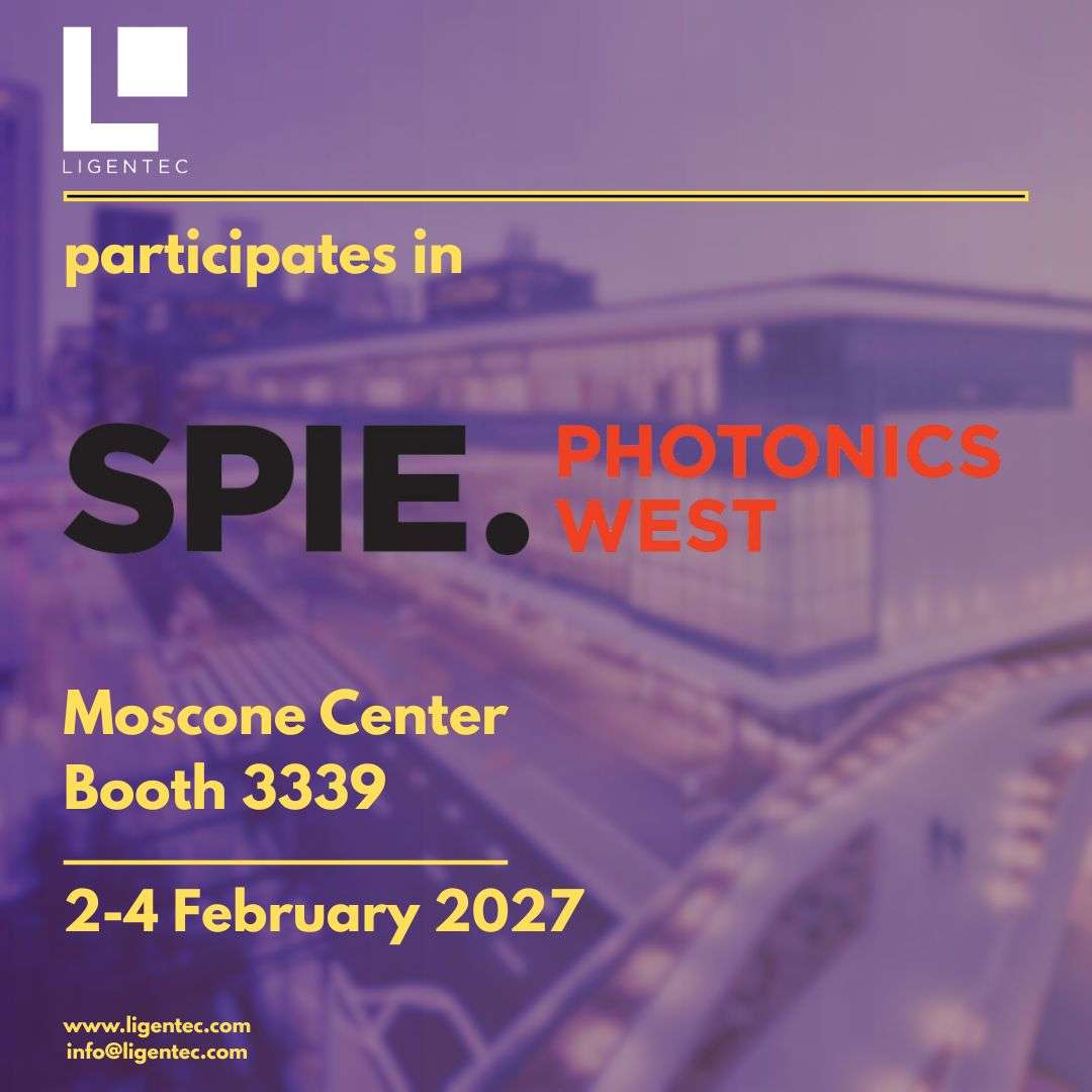
LIGENTEC exhibits at SPIE Photonics West 2027, the leading global event for optics and photonics. Join us in San Francisco from 2 February to 4 February 2027. Visit Booth #3339 to explore our ultra-low-loss Silicon Nitride Photonic Integrated Circuits (PICs).
Meet LIGENTEC at the Photonics West Exhibition
The exhibition runs 2–4 February 2027 at Moscone Center and Moscone West in San Francisco, California. It brings together industry leaders, researchers, semiconductor companies, and photonics innovators.
At Booth #3339, our engineering team will showcase our proprietary Silicon Nitride platform. It delivers the low propagation loss, that sets the industrial benchmark, shipped in every run. In addition, you can watch live demonstrations and speak directly with our process and application engineers. Topics span telecommunications, quantum technologies, LiDAR, and biosensing.
Silicon Nitride PIC Technology at SPIE Photonics West 2027
Our platform supports the most demanding photonics applications. In these applications, optical performance, process repeatability, and scalable manufacturing all matter equally.
Key application areas include:
- Optical communications and coherent transceivers
- Quantum photonics and QKD systems
- LiDAR and advanced sensing technologies
- Biomedical and biosensing applications
Furthermore, we take you from first Multi-Project Wafer (MPW) prototype to 200mm volume production on an automotive-qualified line. Because everything runs within a single 100% European supply chain, your development path scales without supply chain risk.
Why Visit LIGENTEC at Booth #3339
SPIE Photonics West ranks among the most important annual events for the global photonics industry. Optical communications, quantum technologies, imaging, and semiconductor innovation meet under one roof.
Therefore, our team is ready for technical discussions, design consultations, and manufacturing roadmap conversations. Whether you are prototyping your first PIC or planning a volume production ramp, Booth #3339 is where that conversation starts.
Book a meeting in advance: [email protected]