
Europe’s Photonic Integrated Circuits Solution From First Prototype to Volume
Our goal is not simply to process your wafer, but to enable your most innovative photonic products leveraging our mature, high-performance technology portfolio, and accelerate your time-to-market.
As a leading European foundry for Photonic Integrated Circuits, LIGENTEC supports photonic innovation across all global markets. We run our proprietary low-loss SiN manufacturing in an industrial fab, delivering the volume capacity that modern photonic innovation requires.
Where others offer SiN as an option, we offer it as a commitment. Where others stop at the wafer manufacturing, we go all the way to enabling the full solution — with the lowest loss platform, a complete active functionality, and expert support at every step.
Why High-Tech Innovators Win with LIGENTEC
1. The World’s Lowest Propagation Loss in Production
Our proprietary processes deliver the record performance —the industrial benchmark we ship in every run. As the leading pure-play SiN foundry, we provide this performance at scale with the agility and focus specialized applications demand.
2. Active Photonics: A Complete Functionality
We complement the base technology with fast modulators using Thin Film Lithium Niobate (TFLN) and InGaAs photodetectors, integrated directly onto the mature SiN platform.
Our PDK is implemented with leading design tool partners including Luceda, Synopsys, Lumerical, GDSFactory.
3. From Prototype to Production — With Support at Every Step
Your MPW prototypes and volume runs are manufactured within the same production environment in 200 mm automotive-qualified fab. We provide support throughout all stages: from design to testing, packaging and assembly.
4. A European Supply Chain
Switzerland, France, Belgium — prototyping, manufacturing, and design excellence across three locations in Europe. For programmes that cannot afford supply chain risk, we are not an alternative. We are the reference
From Breakthrough to Global Production Standard
Fourteen years. Proven platforms. Zero compromises on loss.
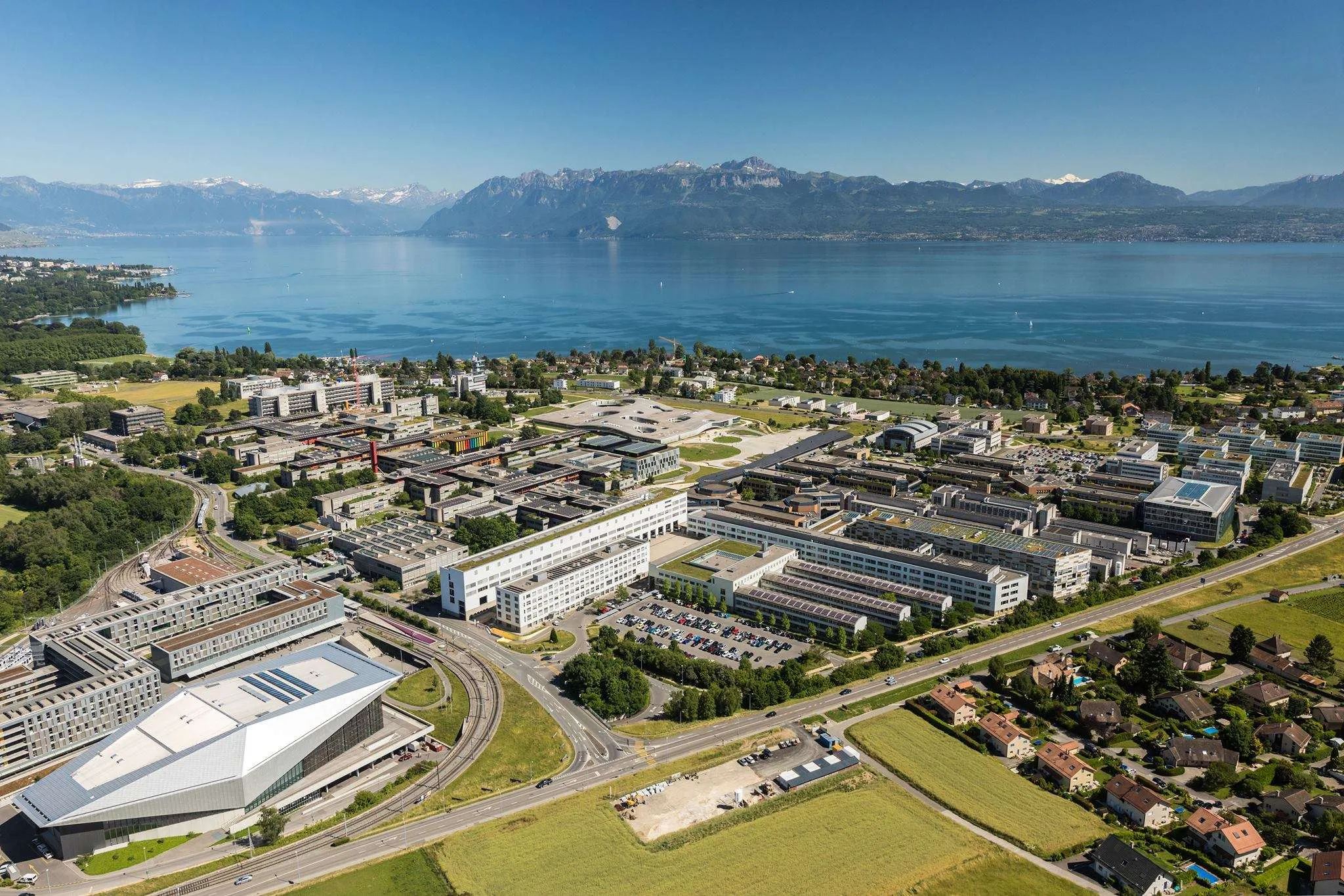
LIGENTEC is incorporated in Lausanne, Switzerland, commercialising state-of-the-art Silicon Nitride photonics manufacturing built on technology development dating back to 2012. A pure-play SiN foundry purpose-built from day one.
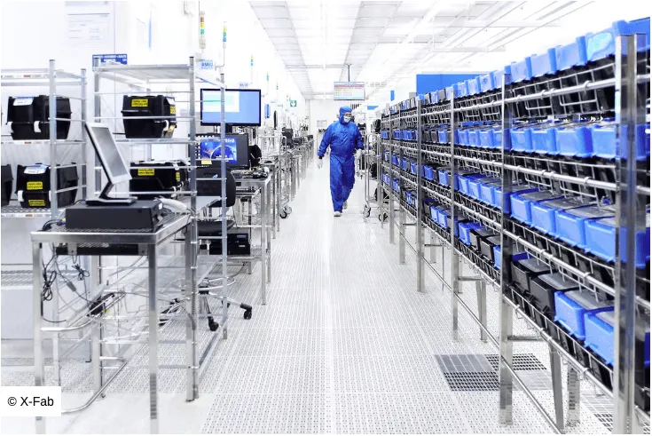
Strategic partnership established with X-FAB, enabling LIGENTEC’s proprietary Silicon Nitride platforms to become available at volume on a world-class, automotive-qualified CMOS manufacturing line, providing a path from prototype to production.
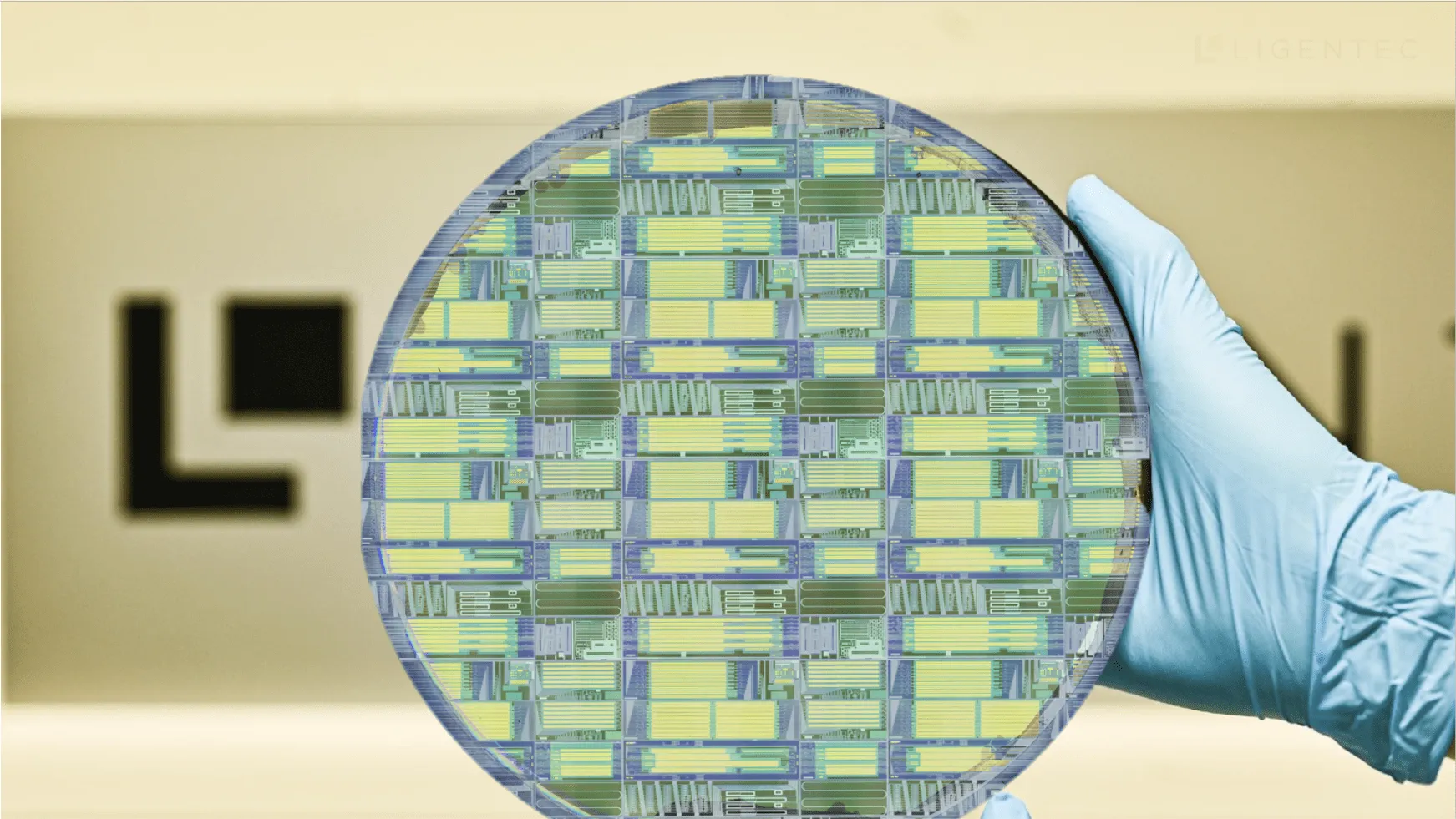
Heterogeneous integration of Thin Film Lithium Niobate demonstrated and commercialised. LIGENTEC becomes the first industrial foundry to offer fast TFLN-on-SiN modulators.

ISO 9001 certification achieved, formalising LIGENTEC’s commitment to quality management and reinforcing its position as a trusted, production-grade foundry partner.
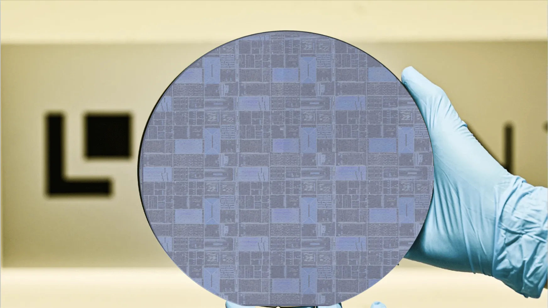
III-V heterogeneous integration demonstrated and commercialised. LIGENTEC introduces InGaAs photodetectors co-integrated with low-loss SiN waveguides, completing the active photonics platform.

LIGENTEC and X-FAB demonstrate a scalable path to heterogeneous integration on mature silicon nitride platforms, jointly investing in its further development — securing the roadmap for next-generation photonic integration at volume.

LIGENTEC expands its offering to Silicon Photonics, serving as the primary customer interface for X-FAB XPH90 SOI platform.
The Enabling Layer for the Most Challenging Applications: Sense, Connect, Compute
Silicon Nitride is not a commodity process. It is the enabling layer for applications where every decibel and every photon matters. LIGENTEC exists to give the engineers, scientists, and programmes working on those problems not just a production-grade process — but a complete path to a design win. From PDK access through design support, testing, and production-qualified volume delivery.
Precision Measurements
Powering applications like light detection and ranging (LiDAR), biosensing, and atomic clocks where every photon brings value.
ConnectBandwidth & Reach
Supporting telecom, datacom, and satellite links with power efficient solutions.
ComputeDemanding Calculations
The platform of choice for optical computing, AI accelerators, quantum processors, and efficient interposers.
Three Locations. One Supply Chain.
30+ nationalities — a team built for the international markets we serve.
Ecublens, Switzerland (HQ)
Design, Process, Test, QCSwiss precision at every stage of development.
Corbeil-Essonnes, France
Design En., Prod., TestMature processes at industrial scale.
Ghent, Belgium
Heterogeneous integrationAdvanced R&D in the heart of the European photonics talent network.