
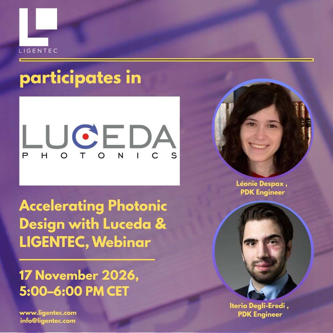
LIGENTEC and Luceda Photonics host a live webinar on accelerating photonic circuit design, November 17, 2026, 17:00–18:00 CET. Both companies are partners in the photonixFAB consortium, the EU-funded project building a European industrial photonics value chain.
45 minutes plus 15 minutes of Q&A. We’ll walk through circuit layout to fabrication-ready verification using LIGENTEC’s Process Design Kit (PDK) in Luceda’s design environment. Register to attend live.
What You’ll Learn
Photonic design and fabrication readiness are usually handled by two separate teams. This webinar covers where teams typically lose the most time in the design-to-tape-out cycle, and the tools that close that gap:
- Circuit Design: Placement and layout using LIGENTEC’s PDK in Luceda’s design tools
- Statistical Models: What’s available and how to apply them to your design
- Design Rule Checking: LIGENTEC’s DRC, run as a Luceda tool, for First Time Right results
Applicable across telecommunications, LiDAR, sensing, and quantum photonics.
Why Attend
Direct access to the engineers building the tools. Bring your questions on:
- Reducing propagation loss in complex circuits
- Working with LIGENTEC’s Silicon Nitride (SiN) platform in Luceda’s IPKISS environment
- Moving a design from first tape-out to production without a redesign
Register to join the live webinar→
Agenda
01 — Welcome & Introduction (5 min) Luceda Photonics and LIGENTEC, and the challenges this partnership addresses.
02 — Live Demo: Circuit Layout to Verification (35 min) Circuit placement and layout in Luceda IPKISS with LIGENTEC PDK, available statistical models, and design rule checking with Irys DRC.
03 — Client Benefits & Takeaways (5 min) Accelerated design cycles, fewer iterations, proven PDK and fabrication access.
04 — Live Q&A (15 min) Ask LIGENTEC’s and Luceda’s experts directly.
From MPW to Volume Manufacturing
Once verified, your design moves through the same platform that takes it to production. Explore Multi-Project Wafer (MPW) runs for cost-effective prototyping, or volume manufacturing on our automotive-qualified 200mm line with X-FAB.
Speakers
Leonie Despax — PDK Engineer, LIGENTEC
Iterio Degli-Eredi — PDK Engineer, Luceda Photonics
Connect With Us
Hear directly from LIGENTEC’s and Luceda’s design and PDK engineers.
Questions? Contact us at [email protected] or [email protected]. We look forward to seeing you online on November 17.