
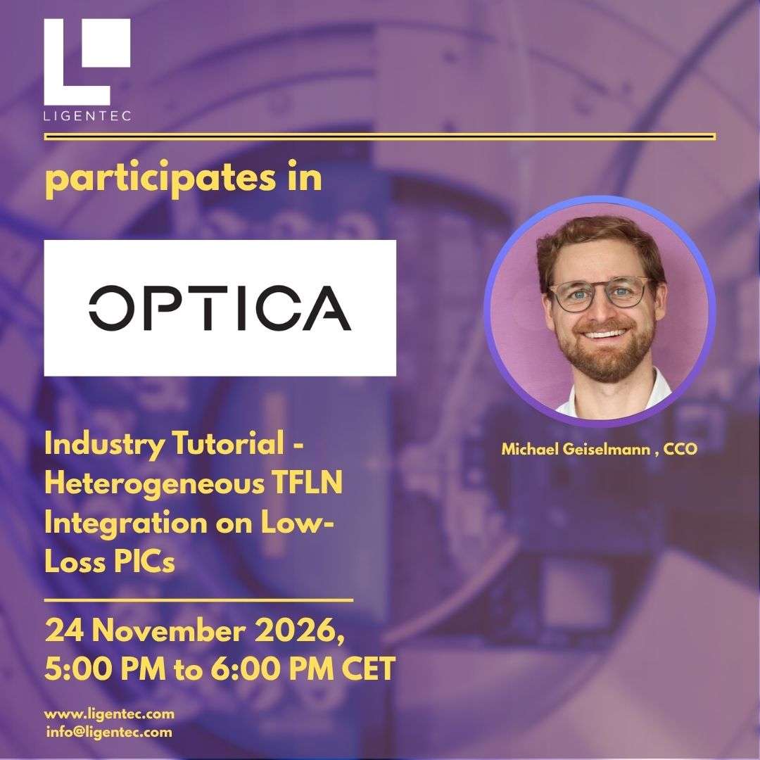
LIGENTEC invites you to an Optica Industry Tutorial on heterogeneous TFLN integration on low-loss silicon nitride (SiN) photonic integrated circuits. Michael Geiselmann explains how to combine ultra-high-speed, low-voltage modulation with an ultra-low-loss waveguide platform, and how this complex process scales from prototype to volume manufacturing.
When: 24 November 2026, 16:00–17:00 CET
Where: Online webinar
Speaker: Michael Geiselmann, CCO, LIGENTEC
Why Attend
Next-generation optical networks need fast, low-voltage modulation and low optical loss on the same chip. Few platforms deliver both. This tutorial shows how LIGENTEC’s heterogeneous platform closes that gap, and how a high-performance prototype becomes a cost-effective industrial product. Whether you design transceivers, sensors or compute engines, you will leave with a clear view of what heterogeneous integration on SiN can deliver for your product. Join this Optica Industry Tutorial online from anywhere, live on Zoom.
What You’ll Learn
- How TFLN on SiN enables low-voltage modulation beyond 110 GHz
- How high-speed photodetectors integrate directly onto the low-loss (dB/m) SiN waveguide core
- How low-loss waveguides enable tunable lasers, comb lasers and efficient fiber-to-PIC interconnect
- How LIGENTEC and X-FAB are transferring this heterogeneous process to a high-volume, automotive-qualified foundry
- Which applications benefit in sensing, communication and computing
From Prototype to Volume Production
Prototyping starts with LIGENTEC’s Multi-Project Wafer (MPW) runs, which let teams validate designs at low cost. Once a design is proven, the same platform carries it to 200 mm volume manufacturing on an automotive-qualified line with X-FAB.
Meet the Speaker
About LIGENTEC
LIGENTEC is a European photonic foundry based near Geneva, offering full-service SiN PIC fabrication from MPW prototyping to 200 mm automotive-qualified volume production. Its platform serves telecom, sensing, LiDAR, quantum and microwave photonics applications.
Register now to secure your place.
Questions? Contact [email protected]